JAKARTA – Changes continue to occur in the chip industry in the world. Apart from making faster and more sophisticated chips with more powerful capabilities, there are other challenges as well.
Siemens Digital Industries Software, a unit of Siemens AG, is making the latest innovations in the chip world. The German company, on Monday, September 26, launched a new piece of software called Tessent Multi-die which automates the design process for testing chips made with advanced packaging.
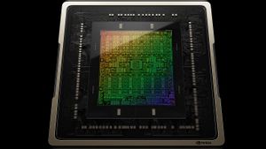
Chips have traditionally been packaged with a single silicon tile inside. Today the chip industry faces the challenge of making the features on these tiles smaller and smaller in order to cram more computing power into them. However, chip companies, including Intel, are now starting to pile on some of them. Sometimes even mix and match different technologies, to improve performance.
But testing these chips once they are made is difficult because there are multiple layers of tiles, and Tessent Siemens head of business, Ankur Gupta, said until now Siemens had to work with customers on a case-by-case basis.
SEE ALSO:
Testing is an important part of the chip and port manufacturing process and to test it must be designed into the chip before it is manufactured.
"What we're doing now is taking all that learning and automating the solution, making it publicly available for everyone to use," Gupta told Reuters.
He said making the testing process easier for chips with advanced packaging, also referred to as 2.5 and 3-dimensional packaging, would help give the new technology a boost.
The English, Chinese, Japanese, Arabic, and French versions are automatically generated by the AI. So there may still be inaccuracies in translating, please always see Indonesian as our main language. (system supported by DigitalSiber.id)


