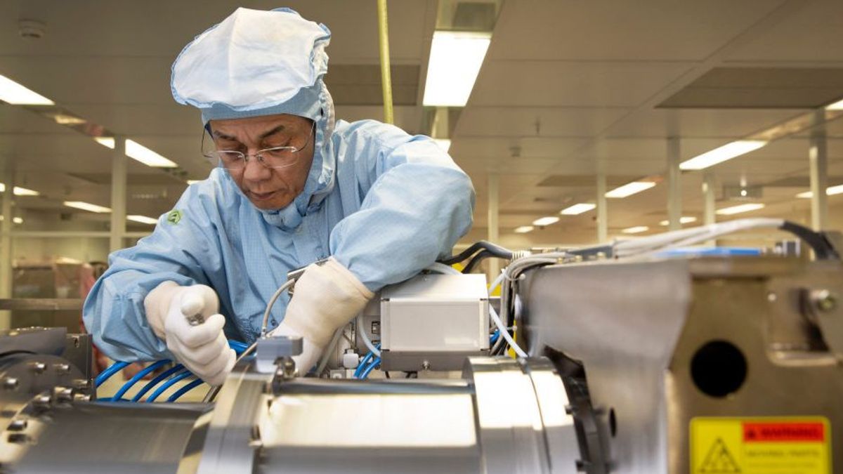


JAKARTA - Huawei has just submitted an application for a one-component patent used in the Extreme Ultraviolet (EUV) Litography system which is useful for making high-end processors at 7nm (nanometers) nodes.
This EUV system is used to improve the creation of integrated circuits and chipsets. Together, this process will form an interference pattern that will continue to change with new light rays.
As a result, this will equalize light exposure and will solve the non-uniform light problems that often occur in chip development.
Along with uniform light rays, this mechanism will facilitate the creation and formation of nanoparticles assembled in integrated circuits or micro-chipsets.
Furthermore, lithography will make transfers, processing, and fabrication of micro-nano graphs. It also verifies the total element completed in the chipset and checks the corresponding sizes and other details on the circuit
The EUV Litography System was currently created exclusively by Dutch company ASML and filed a similar patent (US2016007434A1) in 2016 but has a different scope of patents. ASML is not allowed to sell the machine to China.
The difference between the two patents is that Huawei uses a rotating illumination device to reduce the number of bright or dark patterns in the same area. It seems that Huawei really wants to overcome the vacancy in the EUV Litography market.
As EUV discovery helped bring chips to 7nm and lower process nodes, Huawei patents could help China's Semiconductor Manufacturing International Corporation (SMIC) ultimately compete with TSMC and Samsung Foundry.
Currently, SMIC China is believed to be capable of producing 7nm chips for crypto mining but is limited to 14nm process nodes for smartphone chips.
Meanwhile, ASML allows the same light files to be separated and occur at different points to produce uniform light. On flat panels and relatively moving and stationary reflector sets.
Apparently, the patent of the ASML EUV Litography system relies on the same principle as the older litography shape but uses light with a wavelength of about 13.5nm, which is almost X-ray.
ASML needs more than 6 billion euros equivalent to IDR 99.9 trillion and 17 years to develop the first wave of a sellable EUV Litography system. Launching TechBlog, Tuesday, December 27, but before completion, the United States (US) government pressured the Dutch government to ban exports to China, restricting the country from using older Deep Ultraviolet (DUV) technology.
Currently, only five companies are using or have announced plans to use the ASML EV Litography system, namely Intel and Micron in the US, Samsung and SK Hynix in South Korea, and TSMC in Taiwan.
Chinese companies like Huawei have previously been able to send their designs to factories like TSMC for manufacture with EUV Litography. However, since the US imposed sanctions on China, it has made Huawei even more difficult.
Meanwhile, the company needs access to advanced nodes that use EUV Litography to continuously refine its specialized processors, which target everything from smartphones to data centers. The road is still long before it can create its own EUV Litography system, but they receive a lot of capital and support from the government to achieve it.
The English, Chinese, Japanese, Arabic, and French versions are automatically generated by the AI. So there may still be inaccuracies in translating, please always see Indonesian as our main language. (system supported by DigitalSiber.id)
Most Popular Tags
#Prabowo Subianto #donald trump #2026 World Cup #venezuela #konflik timur tengahPopular


